With the rapid advancements in semiconductor technology, manufacturers continue to introduce new generations of chips with smaller nanometer-scale nodes. TSMC is preparing for mass production of 2nm chips in the second half of this year, while Intel has completed the design and development of 1.8nm chips (Intel 18A) but has yet to begin full-scale production. This raises an important question: Does the term “2nm” actually reflect physical dimensions, or is it primarily a marketing concept representing other improvements?
The Shift from Physical Dimensions to Performance Metrics
In the past, chip node names directly corresponded to the smallest physical dimension on the chip, often referring to the transistor gate length. For example, when manufacturers used 180nm, 90nm, or 45nm process technology, these numbers represented actual measurements of the transistors’ components. However, with ongoing technological evolution, chip structures have become far more complex, making it difficult to describe manufacturing precision with a single dimension.
What Does “2nm” Really Mean?
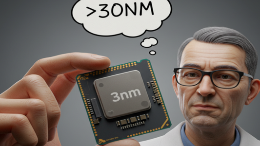
Today, node names such as 7nm, 5nm, 3nm and 2nm no longer represent exact physical dimensions. Instead, they indicate improvements in:
- Transistor density — Increasing the number of transistors packed into a given space.
- Performance enhancements — Faster and more efficient chip operation.
- Power efficiency — Lower energy consumption compared to previous generations.
For example, chips manufactured with a 3nm process do not contain individual components that are precisely 3nm wide. Instead, they represent a new generation of technology that delivers performance gains.
Estimating the Physical Dimensions
While chipmakers rarely disclose the exact measurements of individual components, analysts and reverse engineers estimate dimensions based on metrics like contacted gate pitch (CPP), the metal pitch (The smallest distance between chip components). For instance, 3nm nodes from Samsung, Intel, and TSMC have a CCP ranging between 40 and 50 nanometers and the smallest metal pitch between 22 and 30 nanometers.
Conclusion: A Marketing Term with Technical Significance
Thus, manufacturing labels such as 2nm and 1.8nm are primarily marketing-driven designations, highlighting major advancements in transistor density and overall chip performance, rather than indicating the exact physical size of individual components.