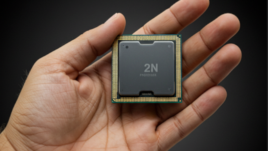
On April 1, 2025, the Taiwanese company TSMC announced the world's most advanced chip: a chip manufactured using 2-nanometer technology, with mass production expected to begin in the second half of the year.
This chip is distinguished from its previous 3-nanometer chips by an increase in computing speed of 10%-15% at the same power level, or a reduction in power consumption of 20%-30% at the same speed.
This silicon chip consists of billions of transistors, and reducing the size of these transistors leads to an increase in their number, thus increasing the chip's speed and reducing the amount of power required for each transistor. The density of transistors in this 2-nanometer chip increases by about 15% compared to the 3-nanometer technology.
TSMC manufactures chips for most global companies, including Apple's processors, NVIDIA's artificial intelligence accelerators, and some of Qualcomm's and AMD's processors. Therefore, many computers, phones, data centers, and artificial intelligence applications can benefit from this technology in achieving better performance and greater energy efficiency.
The company has been developing and testing this technology for several years, as producing such chips requires advanced techniques, including Extreme Ultraviolet Lithography (EUV). This process is very precise and difficult to implement, which increases the cost and time required for production. Furthermore, reducing the size and increasing the density of transistors increases the complexity of thermal management systems to dissipate the generated heat, which can affect the chip's performance and lifespan.
However, the company's ability to overcome all these obstacles and reach the production stage heralds a new generation of smaller and more efficient chips, which will positively impact all electronic devices and AI applications we use.