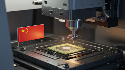
A research team at Fudan University in China has successfully manufactured the first processor chip that uses molybdenum disulfide (MoS2) as a semiconductor material instead of silicon. This material is known for being extremely thin, hence it is called two-dimensional, as chips produced from it can have a thickness of no more than one nanometer, opening new horizons in miniaturizing electronic devices and improving their performance in terms of speed and energy efficiency.
This processor has been named “WUJI,” and its chip measures 6 x 6 millimeters, containing 5900 transistors, thereby breaking the previous world record of 115 two-dimensional transistors on a single chip.
The processor is built on the RISC-V architecture and operates with a 32-bit system. This is the first time an integrated processor capable of executing all instructions of the RISC-V architecture has been built using two-dimensional materials. This architecture is characterized by being open-source, allowing for commercial use without any licensing costs, unlike well-known commercial architectures such as ARM or X86 from Intel.
In the chip fabrication process, the team benefited from many mature silicon manufacturing techniques. However, due to the thinness and sensitivity of molybdenum disulfide, they placed its layers on a sapphire substrate. Furthermore, because it was not possible to use the doping techniques followed in silicon chips for designing the transistors, they adopted new methods based on using fine wires to adjust the threshold voltage.
Subsequently, they connected the transistors to form 25 types of logic gates, which are the fundamental components for performing the necessary arithmetic and logical operations to execute any program. With this, the team is laying the foundations for a new methodology in designing logic gates that is suitable for the connection method of these two-dimensional transistors.
The team has achieved significant success in manufacturing, with an overall yield of 99.8% and a per-chip yield of 99.8%. These percentages are considered excellent, as the overall yield refers to the proportion of working chips among all produced chips, while the per-chip yield expresses the proportion of working components on the chip compared to the total number of components.
This achievement represents an important step demonstrating the feasibility of manufacturing functional processors using thousands of two-dimensional transistors, which is particularly promising given that these technologies are still under development for experimental materials like molybdenum disulfide (MoS2). However, this processor is still in the early stages of research and development and faces significant challenges before it can compete with currently used silicon chips. The size and density of its transistors are still far from the level required for effective commercial applications; a silicon chip of the same size today contains billions of transistors compared to the 5900 transistors in this processor.
However, technological development proceeds in gradual steps, and just as with Intel’s first processor in 1971, which contained only 2900 transistors, this achievement represents a fundamental building block in the advancement of electronics based on two-dimensional materials.
With continued research and development in manufacturing techniques, we are getting closer and closer to fully benefiting from the promising advantages of these materials, such as scalability, speed, and energy efficiency, thus paving the way for the post-silicon era whose features are beginning to become clear today.
The research was published in the journal Nature.