The JFS Laboratory, based in Wuhan, China, has announced a significant breakthrough in silicon photonics. These chips integrate optical technologies with electronic silicon chips, utilizing light instead of electrical signals for data transmission, resulting in higher speeds.
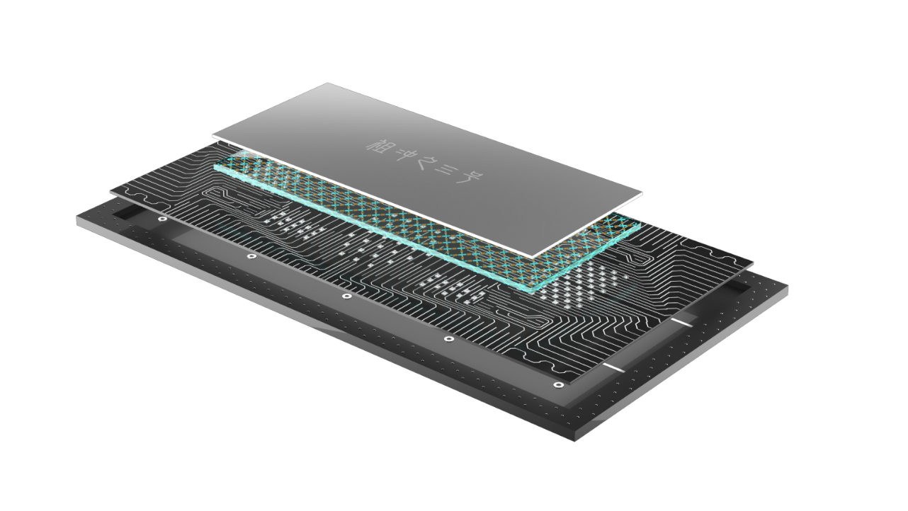
The lab succeeded in integrating a laser light source with a silicon chip, enabling data transmission via light at higher speeds, lower energy consumption, and reduced heat production. Although chip manufacturers outside China had previously achieved this, it is a first for China.
Founded in 2021 with $8.2 billion in government funding, JFS is one of China’s key institutions tasked with technological breakthroughs. Silicon photonics, believed by chip manufacturers, opens new doors in chip production. Major companies investing in this field include the Taiwanese TSMC, Samsung, Nvidia, and Intel.
For China, this is a significant step to circumvent sanctions that restrict access to advanced technologies needed for cutting-edge chip manufacturing. Unlike advanced silicon chip production, which relies on high-end extreme ultraviolet (EUV) lithography machines banned from export to China since 2019, China possesses the tools and materials necessary for silicon photonics.
However, while integrating photonics enhances chip performance, it doesn’t entirely mitigate the impact of semiconductor technology restrictions. China will still require these technologies for the silicon component of the chip.
Transitioning this acheivment from laboratory experiments to mass production and achieving parity with global leaders poses significant challenges. Moreover, silicon photonics, being a relatively nascent technology, may take time to become widely adopted in mainstream applications
