Huawei Launches Mate 90 Series with the World’s First 3D Architecture Processor
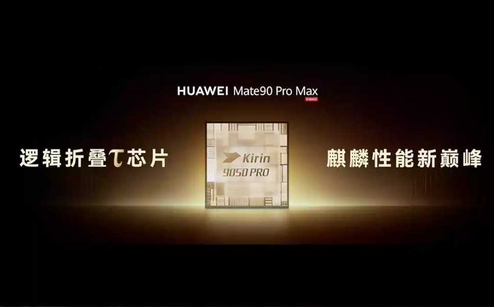
With the launch of the Mate 90 smartphone series—comprising four models: the Mate 90, Mate 90 Pro, Mate 90 Pro Max, and Mate 90 RS ULTIMATE DESIGN—Huawei announced the Kirin 9050 Pro processor for the Pro Max, alongside the standard Kirin 9050. Although the company previously introduced this processor in the Mate XT 2 tri-fold phone, its inclusion in the Mate 90 series marks the first large-scale commercial rollout of its proprietary LogicFolding architecture, which was developed and announced months ago.
The Tau Scaling Concept and LogicFolding Architecture
LogicFolding relies on a broader chip development philosophy that Huawei calls "Tau Scaling." For decades, processor advancement was largely measured by shrinking transistor dimensions and packing more of them into the same area. Tau Scaling introduces a new objective. Instead of the primary question being, "What is the smallest transistor we can manufacture?", Huawei poses another: "What is the absolute shortest time data needs to cross the system?"
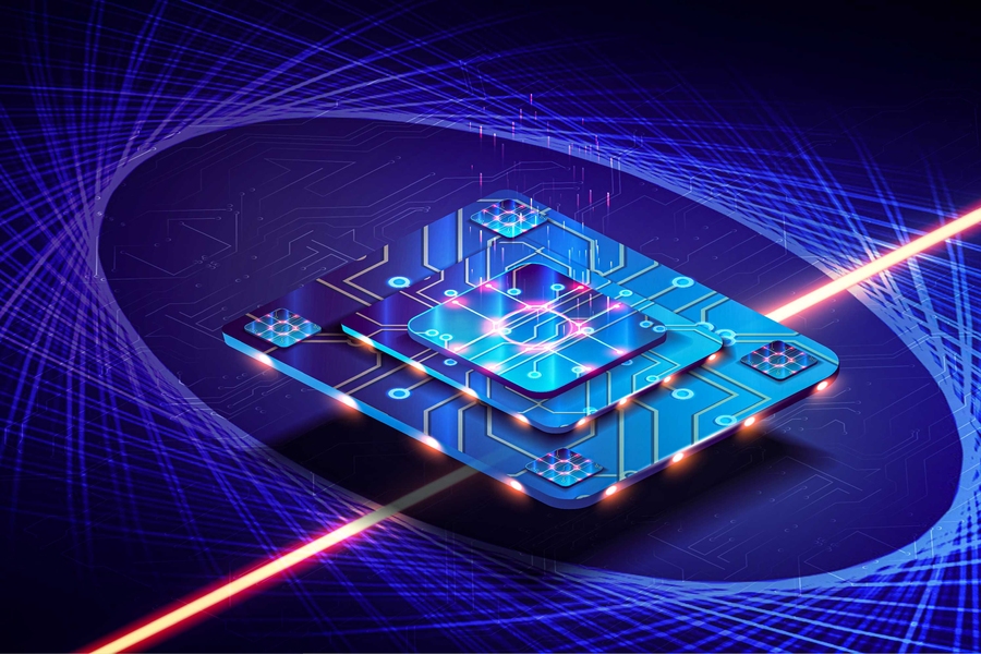
Tau Scaling focuses on reducing signal transmission and processing time by shortening the physical connections between transistors, diverging from the traditional approach that relies primarily on shrinking transistors using advanced manufacturing equipment. This is where LogicFolding architecture comes in. It begins at the circuit design phase by vertically redistributing circuit components. Instead of routing connections over long horizontal distances, sections of the circuit are folded over one another and linked via vertical connections using advanced Hybrid Bonding techniques, creating direct, high-density connections between layers.
Consequently, the third dimension becomes an integral part of the logic design itself, rather than just a method to stack separate chips within a single package, as seen in traditional 3D Packaging techniques. As these pathways shorten, the capacitance and power required to drive the signal decrease, and the need for certain buffer circuits drops. This makes data transfer faster, opening the door for increased performance within the same power and thermal limits.
A Leap in Density and Performance Beyond Manufacturing Constraints
Applying this methodology to the Kirin 9050 processors has yielded significant leaps without relying solely on migrating to a smaller manufacturing node—a step that would require advanced ASML equipment currently subject to export restrictions to China. The new architecture pushes transistor density to roughly 238 million transistors per square millimeter, compared to about 155 million in the previous generation (a roughly 55% increase). This density actually surpasses that of the Apple A18 Pro processor—manufactured by TSMC on a 3nm node—which sits at roughly 190 million transistors per square millimeter.
Alongside this density, the new architecture features over 5 million contact points, an internal bandwidth of around 125 terabytes per second across processor segments, and a 30% reduction in critical path latency. On the performance front, the Kirin 9050 Pro features 9 processing cores and 16 threads with Hyper-Threading technology. The processor registers a 31% higher overall performance compared to the Kirin 9030, boasting a 23% boost in multi-core processing, a 40% increase in graphics performance, and a staggering 140% jump in NPU (AI) performance.
The Future of Processor Engineering Beyond Smartphones
From this perspective, LogicFolding technology is part of a broader shift in processor engineering that supplements continuous miniaturization with vertical stacking. The implications of this technology extend far beyond smartphones. If Huawei can successfully scale this architecture to AI chips and server processors, its utility could be exponential, as data movement between compute and memory units remains one of the largest sources of power consumption and latency in modern computing systems.
If successful, the Kirin 9050 Pro will be viewed as more than just a new generation of mobile processors; it will be the launchpad for the Tau Scaling concept itself, much like Moore's Law drove semiconductor evolution for decades. The future of processor development may no longer rely solely on shrinking the transistor, but on reimagining how transistors and communication pathways are organized in three-dimensional space.