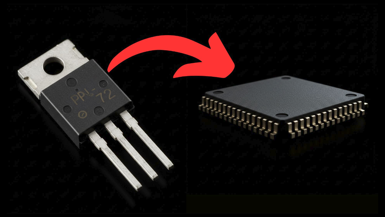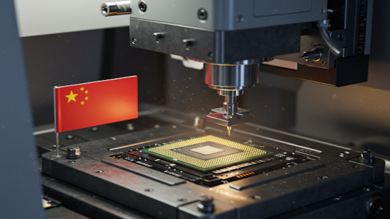
A team of researchers at Peking University has achieved a significant breakthrough in transistor technology (the fundamental component of all electronics). They have successfully manufactured a two-dimensional (2D) transistor that is 40% faster than the latest 3-nanometer technology from Intel and TSMC, while consuming 10% less power.
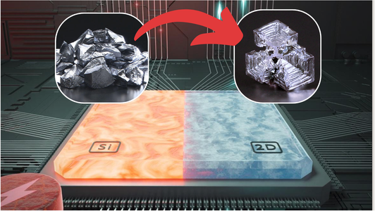
This transistor incorporates innovation at three levels. Firstly, it utilizes bismuth-based materials, such as Bi₂O₂Se as a semiconductor and Bi₂SeO₅ as a high-quality insulating oxide. These materials are ultra-thin, with a thickness of less than 1 nanometer, making their height negligible compared to their length and width, hence they are classified as two-dimensional (2D) materials. In contrast, traditional silicon-based transistors (3D) have reached their miniaturization limits, making further size reduction increasingly difficult. Therefore, relying on ultra-thin materials like bismuth represents a promising direction for the development of electronics.
Secondly, the researchers adopted the GAAFET (Gate-All-Around Field-Effect Transistor) design, but using bismuth-based 2D materials, a modern technology for micro-transistors. This design differs from FinFET (Fin Field-Effect Transistor), developed by Intel and an industry standard since its commercial launch in 2011, which relies on 3D silicon fins. GAAFET surrounds the channel from all sides, making it smaller and more controllable. Therefore, it is used in advanced transistors with 3-nanometer manufacturing processes or smaller.
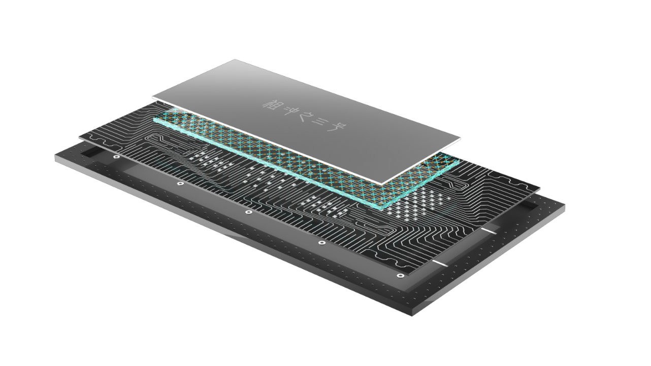
Thirdly, for the 2D transistor to be practical and competitive in the electronics industry, it was essential to find an effective way to stack a large number of these transistors in a small space without sacrificing performance. The Chinese team successfully applied an innovative 3D stacking technique known as “Low-Temperature Monolithic 3D Integration.” This method allows for the alignment of multiple layers of 2D transistors on top of each other on a single chip, while maintaining material quality and high performance. The technique relies on low temperatures to avoid damaging the ultra-thin materials, enabling the production of large quantities of transistors with high density, making it widely applicable in advanced chip manufacturing.
Test results, published in Nature Materials, showed that this transistor is 40% faster (approximately 1.4 times) than the latest 3-nanometer silicon transistors, with a 10% power saving.
This high performance, supported by ultra-thin bismuth materials, GAAFET design, and low-temperature 3D stacking techniques, could revolutionize the future of electronics, transcending the silicon era and opening new horizons for ultra-efficient, low-power devices.